This article is reproduced from WeChat WeChat official account’s "Intelligent Computing Core World" by Hao Zi. Reprint this article, please contact WeChat official account of Intelligent Computing Core World.
ASIC (Application Specific Integrated Circuit) chip is an application-specific integrated circuit, which is designed and manufactured from the root level according to the user’s demand for a specific electronic system. Its computing power and efficiency can be customized according to the algorithm needs, and it is the product of fixed algorithm optimization design. ASIC chip module can be widely used in intelligent terminals such as artificial intelligence equipment, virtual currency mining equipment, consumable printing equipment and military defense equipment.
On the hardware level, ASIC chip is composed of basic silicon material, gallium phosphide, gallium arsenide, gallium nitride and other materials. On the physical structure level, ASIC chip module is made up of IP cores such as plug-in storage unit, power manager, audio picture processor and network circuit. The same chip module can carry one or several ASIC chips with the same or different functions to meet one or more specific requirements.
(1) ASIC chips can be divided into fully customized ASIC chips, semi-customized ASIC chips and programmable ASIC chips according to different customization degrees.
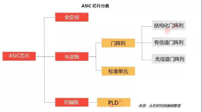
Fully customized ASIC chip is one of the chips with the highest degree of customization. R&D personnel design logic units with different functions based on different circuit structures, and build analog circuits, storage units and mechanical structures on the chip board. The logic units are connected by masks, and the mask of ASIC chip is also highly customized.
The design cost of fully customized ASIC chips is high, and the average design time per chip module exceeds 9 weeks. This kind of chip is usually used for advanced applications.
Compared with semi-customized ASIC chips, fully customized ASIC chips perform well in performance and power consumption. For the same function, under the premise of the same process, the average computing power output of fully customized ASIC chip is about 8 times that of semi-customized ASIC chip, and the performance of fully customized ASIC chip with 24 nm process is better than that of semi-customized ASIC chip with 5 nm process.
Most of the logic units that make up the semi-custom ASIC chip are taken from the standard logic unit library, and some of them are customized according to specific requirements. Compared with fully customized ASIC chips, the design cost is lower and the flexibility is higher.
Semi-custom ASIC chips can be subdivided into gate array chips and standard cell chips according to the different matching modes of standard logic cells and custom logic cells.
A, gate array chip
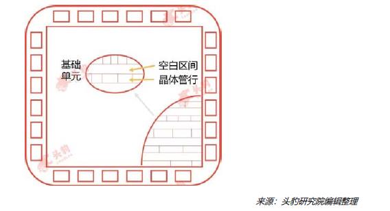
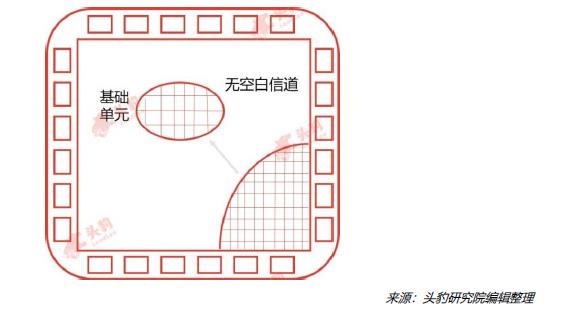
Gate array ASIC chip includes channel gate array, channel-free gate array and structured gate array. In the gate array ASIC chip structure, the predetermined transistor position on the silicon wafer cannot be changed, and designers often adjust the interconnection structure of logic units by changing the metal layer at the bottom of the chip.
Channel gate array ASIC chip: the position of transistors in this chip is highly fixed, and designers can lay out the circuit in the predefined blank space between transistor rows;
Channel-free gate array ASIC chip: under the channel-free structure, there is no circuit layout space between transistor rows, and designers usually wire above the gate array unit;
Structured gate array ASIC chip: This structure includes basic gate array rows and embedded blocks. Embedding blocks can improve the flexibility of circuit layout, but it limits the chip size. Under this structure, the use efficiency of line layout area is higher, the design cost is lower and the turnaround time is shorter.

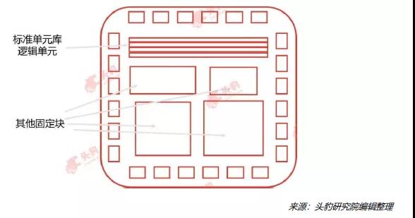
B, standard unit
This kind of ASIC chip consists of logic cells selected from the standard cell library. Designers can arrange standard cells by themselves according to the algorithm requirements. In addition to standard cells, fixed blocks such as microcontrollers and microprocessors can also be used for standard cell ASIC chip architecture.
Broadly speaking, programmable ASIC chips can be divided into FPGA chips and PLD chips. In the actual production process, the number of research institutions and enterprises that classify FPGA chips as different from ASIC chips is increasing, so this report only regards PLD(Programmable Logic Device) as a subcategory of programmable ASIC chips.
PLD, also known as programmable logic device, structurally includes basic logic cell matrix, flip-flop, latch, etc., and its interconnection part exists as a single module. Designers program PLD to meet the needs of some customized applications.
(2) ASIC chips can be classified into TPU chips, BPU chips and NPU chips according to different terminal functions.
① TPU is a tensor processor, which is specially used for machine learning. For example, Google developed in May 2016.
The programmable AI accelerator of Tensorflow platform, its internal instruction set can run when Tensorflow program changes or updates the algorithm.
② BPU is a brain processor, which is an embedded artificial intelligence processor architecture proposed by Horizon Technology.
③ NPU is a neural network processor, which simulates human neurons and synapses at the circuit level, and directly processes large-scale electronic neurons and synapses data with a deep learning instruction set.
Traditional chips, such as CPU, generate results by reading and executing external program code instructions. Relatively speaking, ASIC chips read original input data signals and directly generate output signals after internal logic circuit operations.
(1) Advantages:
Compared with CPU, GPU, FPGA and other types of chips, ASIC chips have multiple advantages in the application of special systems, which are embodied in the following aspects.
① Area advantage: ASIC chips are designed to avoid redundant logic units, processing units, registers, storage units and other architectures, and are constructed in the form of pure digital logic circuits, which is conducive to reducing the chip area. For small area chips, wafers with the same specifications can be cut into more chips, which is helpful for enterprises to reduce wafer costs.
② Energy consumption advantage: ASIC chips consume less energy per computing power than CPU, GPU and FPGA. For example, GPU consumes about 0.4 watts of power per computing power, while ASIC consumes about 0.2 watts of power per computing power, which can better meet the energy consumption restrictions of new smart home appliances.
③ Integration advantages: Due to the customized design, ASIC chip system, circuit and process are highly integrated, which helps customers to obtain high-performance integrated circuits.
④ Price advantage: Due to the characteristics of small size, high running speed and low power consumption, the price of ASIC chips is much lower than that of CPU, GPU and FPGA chips. At present, the average price of ASIC chips in the global market is about $3, and if it reaches mass production scale in the long run, the price of ASIC chips is expected to continue to decline.
(2) Disadvantages:
① ASIC chips have a high degree of customization, long design and development cycle, and the finished products need physical design and reliability verification, so the time to market is slow.
② ASIC chips are highly dependent on algorithms. The high-speed updating iteration of artificial intelligence algorithm leads to the high frequency of ASIC chip updating.
③ Because ASIC chips are highly customized and the research and development cycle is relatively long, the risk of ASIC products being eliminated by the market is expanded.
① Google launched TPU in 2016. Google’s 2017 version of AlphaGo physical processor is embedded with four TPU’s, which can support Google cloud TPU platform and machine learning supercomputer.
② In August 2014, IBM introduced the second generation TrueNorth chip with a manufacturing process of 28 nm by simulating the brain structure, which can be applied to real-time video processing.
③ Intel introduced Xeon series ASIC chips in 2017. This series of chips can act as processors independently, without additional host processors and auxiliary processors, and can be applied to machine deep learning.
④ The ASIC chip based on the new neuromorphological computing architecture introduced by Stanford University is 9,000 times faster than ordinary computers, and can simulate about 1 million brain neurons and billions of synaptic connections.
⑤ Emerging science and technology enterprises expand the application of ASIC chips to security, assisted driving, traditional household appliances, smart medical care and other fields.
The basis for the continuous growth of sales scale of ASIC chip products in China includes but is not limited to the following factors:
① Edge computing field will become the main revenue field of special deep learning ASIC chips.
② Consumer electronic products such as mobile communication devices, head-mounted display devices (AR, VR, MR), tablet computers, drones, smart home devices, etc. will become the concentrated application fields of ASIC chip products.
③ Deep learning processors based on graphics architecture are popular, and ASIC is more suitable for computing environment with graphics architecture.
④ It is predicted that around 2022, artificial intelligence terminal equipment capable of training and reasoning at the same time will become more popular, and ASIC chips will be imported into such equipment in large quantities.
Reference source: China ASIC chip industry boutique report.
关于作者